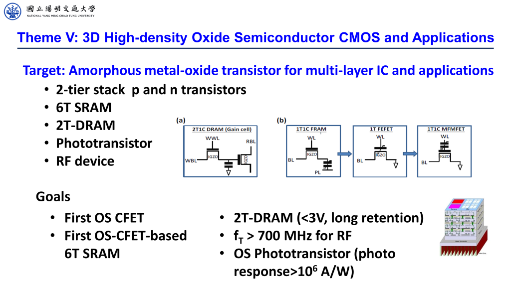
As we move towards the end of Moore’s law scaling, it is critical to explore how to use high-density and low-temperature back-end-of-line (BEOL) process in advanced logic to realize 3D multi-layer stacking of various functional devices (Horizontal 3D; H3D for short). Furthermore, how to realize 3D-NAND-like cost-effective scaling in CMOS by leveraging the development of 3D vertical device structures (Vertical 3D; V3D for short) without needing crystalline channel materials. Oxide semiconductors (OS) have unique advantages in CMOS BEOL process for monolithic 3D (M3D) integration because of their low deposition temperature and ease of processing. Additionally, OS have been widely used in the flat-panel display industry with proven manufacturability. However, the requirements for displays and advanced logic circuits are very different. For example, device size must shrink from micrometer to nanometer. Both N- and P-type materials are required. Reliability requirements become even stricter. The development of a higher-density vertical 3D (V3D) OS device structure does not exist.
We expect to organize a strong research team from NYCU working on advanced M3D-OS research. Our team has more than 10 years research experience on OS. Our team has access to three ALD tools capable of depositing ultrathin OS films. This will provide us with access to various material systems. We also have strong collaboration with both TSRI and ITRI, who can support the integration of nanoscale devices. This project is organized into three thrusts: Thrust 1: ALD amorphous metal oxide semiconductor (AOS) Material Toolbox; Thrust 2: V3D OS-CFET; Thrust 3: Functional OS devices for M3D IC.