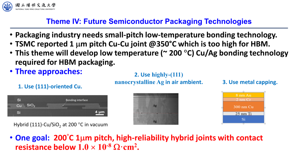
Cu-Cu hybrid bonding has been adopted for high-performance computing (HPC) devices with ultra-high I/O density. TSMC reports that Cu-Cu bonding can significantly increase bump density to 1´106 per mm2, see https://3dfabric.tsmc.com/chinese/dedicatedFoundry/technology/SoIC.htm. Sony has implemented Cu-Cu bonding in CMOS image sensors, and in 2022 AMD has announced the adoption of Cu-Cu joints in high-end processors, such as Ryzen 7 5800X3D [1]. Clearly, Cu-Cu hybrid bonding has become the most important packaging technology for HPC devices. However, the 300 °C bonding temperature is too high for stacking high band width memory devices. With a lower bonding temperature, processes and residual stresses can be more easily controlled. In addition, Cu-Cu joint reliability is still not clear. This project aims to provide solutions and scientific understanding for packaging ultra-high I/O density and enhanced thermal dissipation at lower bonding temperatures or in air ambient. Scaling issues will be also studied.

[1] https://semiengineering.com/next-gen-3d-chip-packaging-race-begins/