The potential applications of ferroelectric materials have been expanded to include the negative capacitance field-effect transistor (NCFET), ferroelectric tunnel junction (FTJ), and ferroelectric field-effect transistor (FEFET). Negative capacitance effects in NCFET devices [1] can reduce gate attack equivalent oxide thickness (EOT), decrease current leakage and increase on-state current or reduce transistor operating voltage and IC power consumption. NC also suppresses short channel effects and can extend channel length reduction. FE memory integrated with NCFET is particularly attractive for density, speed, and process simplicity. A fluorite-type hafnia oxide ferroelectric material, Zr doped-HfO2, such as Hf1-xZrxO2 (HZO) [2], is a strong candidate for next-generation FE devices thanks to its compatibility with the existing CMOS manufacturing technology. It has been proven that ultrathin HZO films (< 2 nm) retain their ferroelectric property [3]. Recently, the EOT of a gate stack consisting of a 1 nm SiO2 interfacial layer (IL) and ~ 2 nm thin HZO is shown to be significantly thinner than that of the IL alone [3, 4]. This is a dramatic demonstration of the novel NC effect. NCFET is important because it may the only new solution that allows for significant future reduction in CMOS voltage and power consumption for a long time to come.
The microstructure of HZO is dominated by three phases: tetragonal (T) P42/nmc, monoclinic (M) P21/c phases, and orthorhombic (O) Pca21 phase; the non-centrosymmetric O-phase content is responsible for the ferroelectricity [5]. Unlike perovskite crystals which gradually lose their FE properties with decreasing film thickness, promising FE properties remain in state-of-the-art HZO as the film thickness is reduced to 2 nm and possibly below. As a result, the realization of FE HZO film for practical applications is a primary objective of this research. When FE HZO is grown on amorphous or polycrystalline substrates it is nominally of a polycrystalline nature. Despite intense study [6-8], the non-uniformity of polycrystalline HZO has been a difficult problem for the device electrical performance and uniformity to overcome. This includes the wake-up effect, fatigue, reliability, and low remnant polarization (Pr) [9,10].
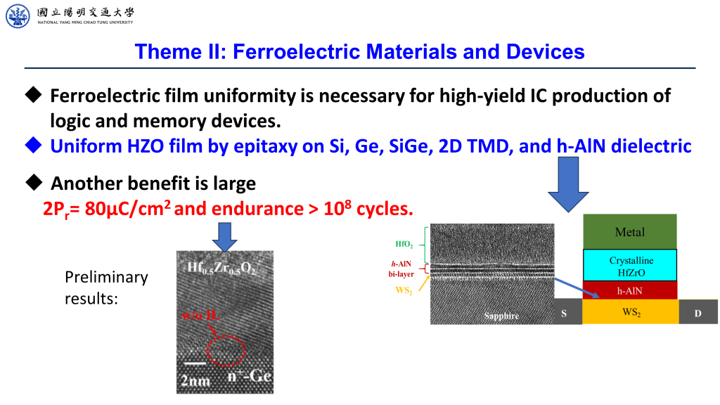
Since pristine HZO film lacks a preferred orientation, FE initialization, also known as the wake-up treatment, is required for device activation and would hinder commercial applications if not addressed. Recent studies have shown that the wake-up problem can be solved by using electrical poling [11,12] and substrate biasing during atomic layer deposition (ALD) [13]. Our previous research has improved Pr, O-phase concentration and wakeup. Using ZrO2-HfO2 interfaces (superlattice) and through optimizing the oxygen vacancy concentration of Hf0.5Zr0.5O2 [14] and T→O annealing [15] favors O-phase formation. However, previously measured 2Pr values ranging from 42 to 72 μC/cm2 [16-18] are considerably less than the theoretical O-phase values [19, 20] owing to the low percentage and the misaligned c-axis of O-phase in polycrystalline HZO films.
[1]. S. Salahuddin et al., Nano Letters 8, 405 (2008). [2]. T. Böscke et al., Applied Physics Letters 99, 102903 (2011).[3]. S. S. Cheema et al., Nature 580, 478 (2020). [4]. S. Jo et al., Nature Electronics published online (2023) [5]. J. Muller, et al., Nano Letters 12, 4318 (2012). [6]. S. J. Kim et al., Applied Physics Letters 113, 182903 (2018). [7]. J. Lyu et al., Nanoscale 12, 11280 (2020). [8]. C. Liu et al., Advanced Functional Materials 32, 2209604 (2022). [9]. Y. J. Lin et al., Applied Surface Science 528, 147014 (2020). [10]. K. Y. Chen et al., IEEE Electron Device Letters 39, 87 (2017). [11]. R. Batra et al. Journal of Physical Chemistry C 121, 4139 (2017). [12]. C. Y. Teng et al., ACS Applied Electronic Materials 5, 1114 (2023) [13]. C. Y. Chou et al., Acta Materialia 228, 117762 (2022). [14]. Z. Zhao et al., IEEEElectron Device Letters 43, 4 (2022). [15]. S. J. Chang et al., Applied Materials & Interfaces 13, 29212 (2021). [16]. M. H. Park et al., Applied Physics Review 6, 041403 (2019). [17]. Y. Goh et al., Applied Physics Letters 117, 242901 (2020). [18]. J. Hwang et al., IEEE Electron Device Letters, 41, 1193 (2020). [19]. S. V. Barabash et al., ECS Transactions 75, 107 (2017). [20]. R. Materlik et al., Journal of Applied Physics 117, 134109 (2015).