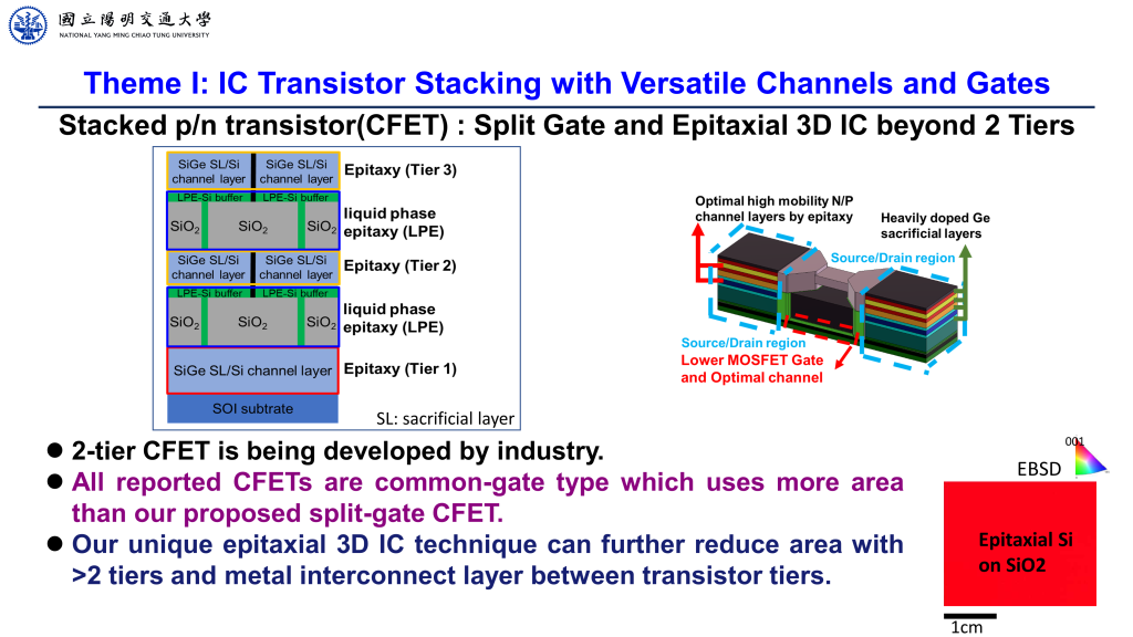
As the semiconductor industry strives to achieve technology nodes beyond 3 nm, the transition of transistor architecture from FinFET to stacked nanosheets is expected for better performance, power, and area due to the improved short channel control by the gate-all-around (GAA) structure and the improved drive current with stacked channels at a fixed footprint. Furthermore, new transistor stacking architecture of CFET can enable inverter cell height scaling and keep driving the Moore’s Law. According to IMEC’s transistor roadmap extension [1], CFETs could potentially be used in A5 node by 2032.
Monolithic transistor stacking is a viable approach for cell area scaling. For instance, Intel has already demonstrated the successful integration of stacked nFET nanosheets on pFET nanosheets with a common gate structure [2]. Monolithic transistor stacking not only provides self-aligned property to achieve maximum area scaling but also delivers cost reduction advantages over sequential processing, which requires wafer bonding and subsequent substrate removal process. Enhancing the flexibility in transistor stacking allows for the independent optimization of both channel mobility and gate stacks to achieve various circuit applications. For low-power devices, identical channel material of Si can be used for both nFET nanosheets and pFET nanosheets, while for high-performance devices, Ge channels (pFET), and Si channels (nFET) can be integrated [3]. In fact, Intel has reported the implementation of transistor stacking, where Ge nanosheets are fabricated on Si FinFETs sequentially by wafer bonding.
[1] IMEC, Future Summits 2022. [2] C.-Y. Huang et al., IEDM, 2020. [3] W. Rachmady et al., IEDM, 2019.